EDS for TEM Explained
This document gives an introduction to EDS applications in the Transmission Electron Microscope (TEM).
 オックスフォード・インストゥルメンツー事業部ページ

This document gives an introduction to EDS applications in the Transmission Electron Microscope (TEM).
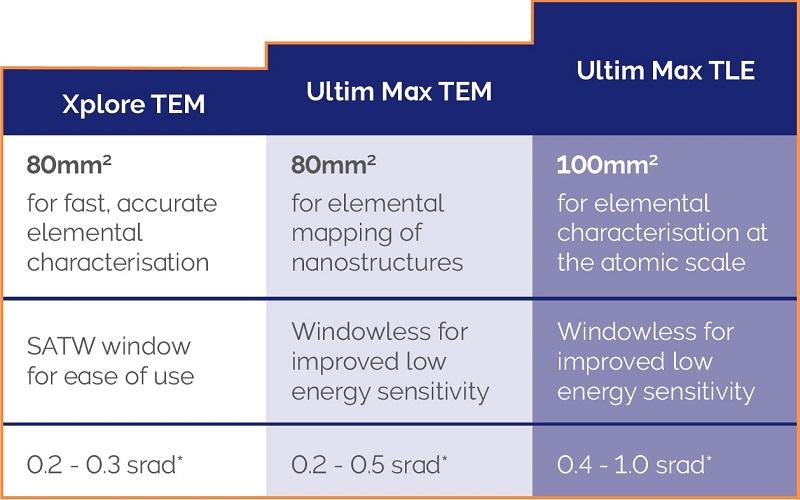
This brochure shows why AZtecTEM is the most powerful solution for EDS on the TEM.
Simultaneous acquisition of EDS and EELS is a powerful tool for materials analysis
Development and testing of semiconductor devices requires extensive knowledge of local structure and elemental composition.
Simultaneous acquisition of EDS and EELS is a powerful tool for materials analysis
Development and testing of semiconductor devices requires extensive knowledge of local structure and elemental composition.

© オックスフォード・インストゥルメンツ 2026